Analog interfaces
This chapter gives more detailed information about the analog interfaces of the 3rd generation MLA™.
The two signal output ports and the four signal input ports are controlled in the MLA GUI via the analog panel.
signal outputs
OUT 1 and OUT 2 are two high speed outputs with 500 MSam/sec and 16 bit resolution. These ports are are always differential and biploar. The output voltage will appear between the + port and ground (SMA shield). The same same voltage with the opposite sign appears between the - port and ground. Therefore, if you use these ports differentially, the voltage difference between and + and - ports will be twice the set value. These ports have 50 Ohm output impedance and they have two ranges:
± 2 V range, maximum current 50 mA.
± 12 V range, maximum current 350 mA.
Caution
The 12 V range is rather powerful and you can burn stuff with it. Be careful with what you are driving when using the 12 V range on these ports.
signal inputs
IN 1 and IN 2 are high-speed (250 MSam/sec) with 14 bit resolution. IN 3 and IN 4 have moderate speed (50 MSam/sec) with 16 bit resolution. All ports can measure either differential or single-ended signals. When measuring single-ended the - input sees an open circuit (but the - input amplifier is grounded internally). All ports have switchable range settings, AC or DC coupling, 50 ohm or 1M ohm input impedance. Making the optimal measurement involves managing trade-offs that effect the noise, gain, bandwidth and intermodulation distortion. You should test different configurations of the MLA™-3 analog interface to see what works best for your measurement.
You can configure the signal inputs from the MLA GUI via the analog panel. When using the analog panel in the Configuration mode, the check boxes under Manual switch control display the state of the input relays. To control the input analog interface in your own program via the MLA API, use the function hardware.Hardware.set_input_relay(), setting every input argument (switch name) to its the desired state, as described in the table below.
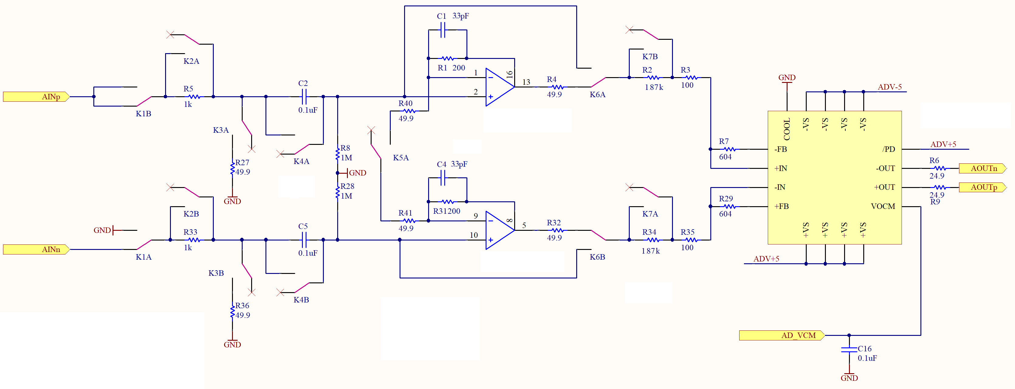
Switch Description |
Schematic |
API name |
state=True |
state=False |
|---|---|---|---|---|
Signal Type |
K1 |
se |
single ended |
differential |
Series Resistance [1] |
K2 |
nodamp |
no series R |
1K series R |
Input termination |
K3 |
term |
50 ohm |
1M ohm |
AC/DC Coupling |
K4 |
dc |
DC coupling |
AC coupling |
1st stage gain |
K5 |
gain |
x 1 |
x 5 |
Bypass |
K6 |
bypass |
bypass 1st stage |
use 1st stage |
2nd stage gain |
K7 |
gain2 |
x 5 |
x 0.5 |
aux outputs
OUT A to OUT D are four slower ports are controlled by a single four-channel DA-converter with a combined speed of 800 kSamp/sec and 16 bit resolution. OUT A is differential, so that a negative copy of the voltage is put between the - port and the shield. When used differentially OUT A will supply twice the value of the set voltage. Each port is driven by an operational amplifier with only one output range:
± 12 V , maximum current 70 mA.
Trigger Output
The trigger output ports are driven by active level shifter circuits for digital signals. The level shifter can be configured to 5 V, 3.3 V or 2.5 V voltage standards by an on-board jumper. The same jumper is used to set the voltage standard for all trigger input and output ports. Trigger output ports have 50 Ω output impedance and are capable of driving 50 Ω inputs at the other end.
Trigger Input
The trigger input ports are connected to active level shifter circuits for digital signals. The level shifter can be configured to 5 V, 3.3 V or 2.5 V voltage standards by an on-board jumper. The same jumper is used to set the voltage standard for all trigger input and output ports. The trigger input ports have high input impedance, which is common for trigger circuits. If you have trouble with reflections in long cables, use an T-connector with a 50 Ω terminator at the trigger input port. If you use the T-connector solution, remember to verify that the trigger output at the other end can drive the 50 Ohm load.
Clock Reference

The reference clock ports are AC-coupled.
The voltage to the REF CLK IN port should be 0.25 to 2.4 Vpp.
The type of the REF CLK OUT signal can be modified from the software, see hardware.Hardware.set_clkout_type().
To set the frequecy of the REF CLK OUT port, see hardware.Hardware.set_clkout_divisor().
To set up the REF CLK IN to lock to an external 10 MHz input, see hardware.Hardware.set_clkref_external_10MHz().
To set the frequency that the REF CLK IN should lock to, see functions hardware.Hardware.set_clkin_parameters().